Author(s): <p>Tsu-Ting Lee, Kashi Chiranjeevulu, Chih-Hsuan Hu, Sireesha Pedaballi, Ching-Ting Lee, Chang-Fu Dee and Edward Yi Chang*</p>
Molybdenum disulfide (MoS2) transistors are emerging as an exciting material system for future electronics due to their unique electrical properties, two-dimensional (2D) nature and atomically thin geometry. This ultra-thin-body (UTB) semiconductor considerably reduces current leakage and enables gate-to-channel control. The homogeneous growth of sub-10 nm dielectrics on 2D materials remains challenging. We demonstrate high-performance MoS2 FETs at low temperature (150°C) using the plasma-enhanced Atomic layer deposition (PEALD) technique. The device exhibits a high on/off current ratio of about 106, the field-effect mobility of 9.5 cm2/Vs, and a subthreshold swing (SS) of 171 mV/dec, which is comparable to the similar structure of the top gate device. In addition, we have demonstrated contact resistance on back-gate MoS2 FETs with and without dielectric capping.
Metal-oxide-semiconductor field-effect transistors (MOSFETs) scale beyond Moore’s Law and offer several advantages like low operating voltages, faster-switching speed and virtually no input current required to control the load current. There is vital need to develop alternative semiconductor materials and technology to overcome short channel effects. As MOSFETs reach sub-10 nanometer channel lengths, an ultra-thin-body (UTB) semiconductor can reduce gate leakage current while providing an effective electrostatic coupling between the gate and semiconducting channel. For effective gate coupling of the device, the semiconductor thickness should not be more than or equally 1/3 of the gate length [1]. In sub-5 nm gate lengths, this channel materials with only 1 or 2 atomic layers in thickness. Due to their essential thickness uniformity and ability to become a monolayer, two-dimensional (2D) semiconductors are excellent candidates for the channel material of future single layer-FETs. Exfoliation of graphene has led to the development of two-dimensional (2D) materials. As a promising alternative to silicon, graphene exhibits superior carrier mobility of up to 200000 cm2/V, but its lack of bandgap severely limits its use in digital logic. In contrast to zero bandgap graphene, molybdenum disulfide (MoS2) is a semiconducting transition metal dichalcogenide (TMDCs). Having a relatively wide bandgap has shown promise for a variety of applications, including photodetectors [2], flexible electronics [3], low-voltage field-effect transistors (FETs) [4], and monolithic 3D CMOs [5], which is potentially applicable to future flexible electronic and nanoscale devices. Crystals of MoS2 are sticking by van der Waals forces. The single-layer MoS2 has a thickness of 6.5Å. As a result of the ultrathin nature of the material, the high contact resistance (Rc), which controls drain current, a metal/ semiconductor interface will have a high Schottky barrier height [6]. Metal contact layers, Fermi de-pinning layers and doping engineering are necessary to obtain low-resistance contacts [7-12]. Several research groups have recently demonstrated single or multilayer MoS2 FETs using high-dielectric-constant (high-k) materials as top-gate dielectric layers formed by atomic layer deposition (ALD) [13-15]. Despite this, uniformly depositing sub-10nm dielectrics on 2D materials remains challenging since the MoS2 basal plane is free of dangling bonds or functional groups. It is necessary to fabricate large areas of ultra-thin and pinhole-free high-k dielectrics to fabricate MoS2 devices with high performance. Due to the physical adsorbing nature of ALD precursors, Liu et al. claim that Al2O3 can be formed on MoS2 surfaces at temperatures below 200°C compared with chemical adsorption [25,16]. The high-k dielectric engineering plays a key role in MoS2 field-effect transistor (FET) [14-17] Coulomb scattering in dielectrics with high-k values is inhibited by electric field penetration and by mismatches between dielectric constants of nanoscale semiconducting materials [18]. As a result, carrier mobility can be substantially increased. Additionally, the dielectric on MoS2 may reduce hysteresis of FETs by preventing moisture absorption from ambient air and ensuring best performance by integration of high-k gate dielectrics on MoS2 surfaces with atomic layer deposition (ALD) remains a challenge so far [19-21]. ALD is a self-limiting reaction that requires the initial precursor to react uniformly with the sample surface [22]. Because of the chemically inert basal plane of MoS2, utilizing ALD to grow dielectrics easily exhibit poor coverage and discontinuous island-like growth, which will induce a substantial gate leakage. Most MoS2 transistors feature a relatively thick (typically >10 nm) top-gate dielectric, resulting in complete coverage [14,23,24]. Realizing high-quality pinhole- free and ultra-thin high k dielectrics over a large area on MoS2 is an important step towards the practical implementation of MoS2 devices with optimized performance. Liu et al. found that Al2O3 can be uniformly formed on MoS2 surfaces at temperatures below 200°C because the physically adsorbing nature of ALD precursors on MoS2 has a much weaker binding energy than chemical adsorption [25]. The electrical properties of the high-k film will inevitably degrade with decreasing ALD temperatures due to the appearance of impurities or defects such as pinholes [26]. Various methods have been investigated to achieve uniform growth of high-k materials on MoS2, such as surface functionalization methods and ultrathin buffer layers. They have some significant drawbacks when it comes to achieving uniform growth. In some cases, surface functionalization can damage the MoS2surface, causing the devices to perform poorly. Making functional MoS2 FETs requires a stable and effective method of depositing high-quality high-k dielectrics on MoS2. to overcome this issue, we report on the experimental demonstration of Plasma Enhanced Atomic Layer Deposition (PEALD) to demonstrate MoS2 FETs with AlN/Al2O3 as the top-gate dielectric. As a result of the aluminum nitride (AlN) interfacial layer, the gate dielectrics thickness can reduce to as low as 6 nm. We evaluated the electrical stability of the devices under various conditions. Despite huge gate biases and high temperatures, there is small hysteresis. We achieve this result due to the low density of border traps near the MoS2/ Al2O3 interface, small gate leakage, and high dielectric strength of AlN/Al2O3. According to the results, the PEALD process is an excellent way to grow ultra-thin high-k dielectrics to improve the performance of MoS2 FETs [27].
We prepare a few layers of MoS2 using mechanical exfoliation from bulk MoS2 (SPI supplies, USA). After the exfoliation process, MoS2 was transferred to the substrate using thermal tape and with the help of an optical microscope we can determine the number of layers. MoS2 flake with 5 to 15 layers (3.5 nm to 10 nm) has better electrical properties. In this process, we used PEALD method to achieve uniform growth of high-k dielectric material on MoS2 [28-30].
We prepared a P++ Silicon wafer (Electric resistivity: 0.001-0.005 ohm-cm) and deposited SiO2 , 270 nm at temperature range 1000°C by using oxidation and diffusion furnaces (SJ-CA1200-D4). MoS2 and other 2D materials can be optimized by an optical microscope observing the SiO2 thickness. After SiO2 deposition, a wafer clean is necessary to remove chemical residues. Wafers were immersed in acetone and subjected to ultrasonication for about 5 minutes. After soaking in isopropanol (IPA) for three to five minutes, the residual solvent can be removed with N2. After that, the device was fabricated using photolithography and AZ5214E photoresist. JBX-6000FS, E-beam lithography system used in the fabrication process. Photoresists such as PMGI and GL2000 works with E-beam (electron beam) lithography for ohmic metal deposition. For determining MoS2 thickness, we used atomic force microscopy (AFM) (see Supplementary Figure S1) and Raman spectroscopy. A Keithley 4200 was used to measure leakage of the MoS2 gate. Interface evaluation between ALD Al2 O3 and MoS2 crystals, also used for CV measurements. TLM is a technique used to determine the contact resistance between a metal and a semiconductor to study the effects of AlN and Al2 O3 capping on n-type few-layer MoS2 transistors.

Supplementary Figure S1: (a) Microscopic (optical) image of multi-layer MoS2 flake after being transferred to Si substrate capped with SiO2 . (b) AFM image of MoS2 surface after the direct deposition of 6-nm Al2 O3 at 150°C at 4 to 11 layers of MoS2 films on SiO2 /Si from mechanical exfoliation. AlN was deposited by using trimethylaluminum (TMA) and remote N2 plasma (with controllable N2/H2/Ar composition and adjustable RF coil power) as Al and N sources respectively. During one cycle of AlN growth, 40 ms TMA with carrier gas of 10 sccm Ar is provided for the Al source first, then the chamber is purged by 30 sccm Ar for 3 s. Considering that only 20 ms TMA dosage was used for ALD Al2 O3 and had already resulted in a growth rate of 1 Å/cycle, 40 ms TMA for ALD AlN can be regarded as over dosed. 60 s and 20 sccm N2 plasma with an adjustable Ar/H2 content and remote RF coil power is used as N source
AlN was deposited by using trimethylaluminum (TMA) and remote N2 plasma (with controllable N2/H2/Ar composition and adjustable RF coil power) as Al and N sources respectively. During one cycle of AlN growth, 40 ms TMA with carrier gas of 10 sccm Ar is provided for the Al source first, then the chamber is purged by 30 sccm Ar for 3 s. Considering that only 20 ms TMA dosage was used for ALD Al2 O3 and had already resulted in a growth rate of 1 Å/cycle, 40 ms TMA for ALD AlN can be regarded as over dosed. 60 s and 20 sccm N2 plasma with an adjustable Ar/H2 content and remote RF coil power is used as N source.
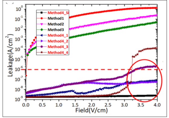
Supplementary Figure S2: The leakage characteristic comparison of the dielectric grown by 4 kinds of the ALD methods
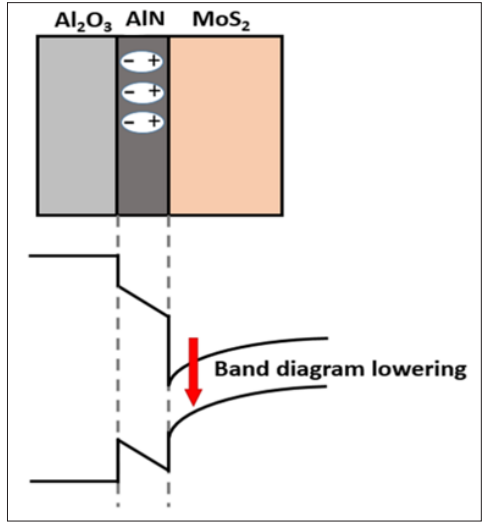
Supplementary Figure S3: The polarization of AlN induced MoS2 band diagram lowering
Here in MoS2 samples were mechanically exfoliated from bulk MoS2 and placed on sapphire substrate by thermal tape. MoS2 flakes were identified under an optical microscope by their color, based on thickness-dependent and optical contrast. The number of MoS2 layers ranged from 5-15 layers (3.5nm -10nm) [33,34]. (See optical and AFM image Supplementary Figure S1). Fig.1a shows the schematic structure of the MoS2 sample after the deposition of 1-nm A1N and 6-nm Al2O3. The surface morphology was characterized by AFM (Figure S1.b) and we observed the resulted a continuous smooth surface. In our experiments, the bare SiO2/Si wafer usually had smoother surface roughness than after the sample was deposited to the SiO2/Si wafer. The weak adhesion of the precursors (TMA, H2O) on the dangling band- free MoS2 surface leads to cracked areas in the dielectric film, which agrees with previous reports [35,36] Although organic solvent residues support the deposition of dielectric materials on MoS2 [22] the failure of direct deposition of Al2O3 on the MoS2 sample also reflects that the MoS2 has maintained a clean surface during the fabrication process. The successful deposition of AlN/Al2O3 on MoS2 could be the result of the relatively low growth temperature of AlN. However, we found that even when the ALD growth temperature of Al2O3 was reduced from 250°C to 150°C, similar poor quality was still observed when Al2O3 was directly deposited on MoS2. Supplementary Figure S2 shows the leakage characteristics of four various ALD methods and the measurement setup for a MoS2 MOSFET device. Thus, we conclude that the improved surface morphology and quality of AlN/Al2O3 dielectric stack on the dangle-bond-free MoS2 surface is mainly the benefits of the low-power remote nitrogen plasma treatment during the PEALD growth of AlN, which is similar to the O2 plasma functionalization of the multilayer MoS2 that was used to promote the ALD deposition of Al2O3 [25]. Even though the remote pure N2 plasma is very mild to single-layer MoS2 during several hours treatment. However, after fine-tuning ALD, it was still possible to reduce the ALD growth temperature of Al2O3 to 150°C at 4 MV/cm2, gate leakage drops to 1000 pA/ cm2 significantly below the acceptable level for Nano-electronic devices and circuits. Surface pretreatment of MoS2 allows it to undergo functionalization without oxidation or damage to the crystal lattice [37,38]. Surface pretreatment does not improve the quality of the oxide sufficiently. Plasma exposure conditions grown by plasma-enhanced ALD at 150°C on MoS2, indicating good growth.
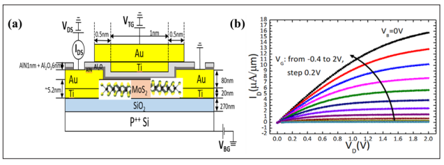
Figure 1: (a) Schematic of MoS2 sample after the deposition of AlN/Al2O3 (b) The transfer curve for the MoS2 FET transistor under different drain voltage biases, the MoS2 FET device with 1 nm AlN and 6 nm Al2O3 gate dielectric
The on/off ratio is high at 107 is achieved, but the resolution of the equipment limits the off-current. The field-effect mobility can be calculated as 9.5 cm2 /Vs using the equation below.

[where L=2 μm and W=6.3um are the channel length and width, respectively].
We investigated the electrical properties of 6 nm Al2O3 and 1 nm AlN ultra-thin dielectrics using low-temperature PEALD. According to Figure 1c, the black and green curves represent the results for stepping VG up and VG down, respectively. ID-VD
characteristics and transfer curves of top-gated MoS2 FETs shown in Figure 2a. The maximum drain current (ID max) is 16 uA/um at VG=2V. As the output curves are linear, the Ti/Au contacts are ohmic, similar to a small drain voltage range, Figure 2b shows the transfer characteristics measurement (ID-VG). previously in a similar structure of a top gate MoS2 FET with 1 nm AlN and 5 nm Al2O3 gate dielectric [39] Despite this, our device only has a sub-threshold slope of 171mv/dec, which may be due to improved oxide interface quality by a lower temperature ALD process and TMA pretreatment. By physically adsorbing precursors onto MoS2, the dielectric is deposited at a low temperature, preventing thermal damage to the channel. A few cycles of TMA molecules passing through the carrier gas (Ar) before A1N deposition increases the number of nucleation sites on MoS2. For gate electric fields as high as 4mV/cm, the top gate leakage current is 10 pA/m2 (see Figure 2c). The gate leakage curve was smaller [40] after resolving the equipment. In both cases, the AlN interlayer and the low- temperature PEALD approach are highly effective in uniformly growing ultra-thin dielectric on MoS2.
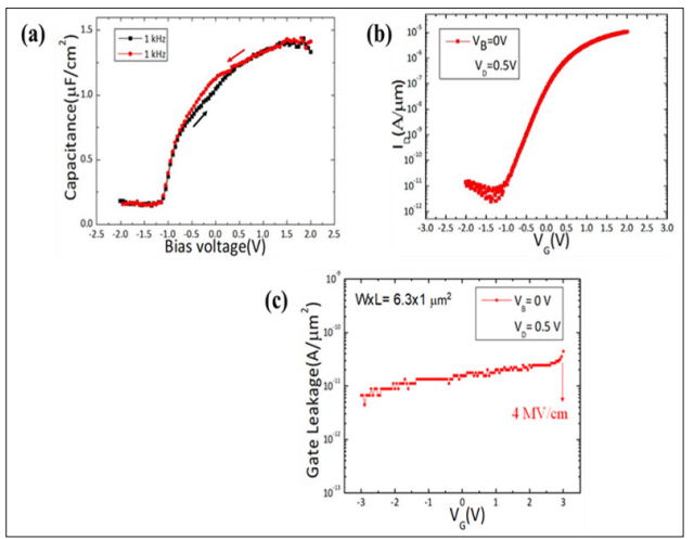
Figure 2: (a) The CV characteristic of the MoS2 FET capacitor with 1 nm AlN and 6nm Al2O3 gate dielectric. (b) The transfer characteristic of the top-gated MoS2 FETs with 1nm AlN and 6 nm Al2O3 gate dielectric. The top gate bias (VG) swept from -2.5 V to 0 V, and the drain voltage was 0.5 V (c) Leakage currents of MoS2 FETs with 1 nm and 6 nm gate dielectrics, respectively.
The Transmission line measurements were conducted on n-type few-layer MoS2 transistors with and without dielectric capping to understand the effects of AlN and Al2O3. As shown in Figure 3a, the contact resistance has been significantly reduced from 95 k Ω•μm to 3.6 k Ω•μm after the dielectric capping. Increased resistance (Rc) may be due to the reduction of Schottky barrier height and decreased dielectric capping. The alignment of bands on a semiconducting 2D crystal determines the polarity of a transistor. A dielectric coating was applied to the surface to reduce contact resistance. We expect AlN’s polarizability to attract electrons towards MoS2. As a result of negative charges accumulating, the MoS2 band will bend (see supporting information S3). By reducing the effective barrier height for electrons, band bending facilitates the injection of electrons from the metal into the conduction band by thermal tunneling. Along with the reduction of the contact resistance, the sheet resistance has also declined from 1×10⁶ Ω/μm to 1.76×10⁵Ω/μm. Figure 3b illustrates that the reduced resistance (Rc) enhances the ID of 0.2μm channel length from 0.22μA/μm to 160 μA/μm at VD = 2V. The drain current (ID) increases more than 700 times. We compared the drain current and contact resistance of short channel back-gate MoS2 FETs (see supporting information S4). Despite this, the contact resistance of 3.6 kΩ•μm is still seven times higher than the previously reported value of 0.5kΩ•μm [12].
Our study revealed that a high contact resistance and low drain current for MoS2 FETs; however, further understanding of the device doping remains. on semiconducting 2D crystals, transistor polarity is more likely to be determined by the band alignment at the metal contacts. After applying the dielectric coating, contact resistance decreased significantly. We believing that AlN’s polarizability will attract electrons to MoS2. As a result of the accumulation of negative charges, the band will bend (see supporting information S3). The band bending reduces the effective barrier height for electrons, making it easier for electrons injected from the metal into the conduction band by thermal tunneling. In addition to the reduction of contact resistance, the sheet resistance has dropped from 1×10⁶ Ω/μm to 1.76×10⁵Ω/μm. As shown in Figure 3b, the reduced resistance (Rc) enrichments the ID of 0.2 μm channel length from 0.22 μA/μm to 160 μA/μm at VD = 2V.
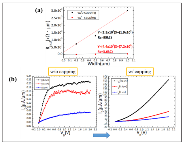
Figure 3: (a) TLM resistances of backgated MoS2 FETs with and without 1 nm AlN and 6 nm Al2O3 gate dielectric caps. (b) A comparison of the ID-VD characteristics of back-gated MoS2
FETs with and without gate dielectric capping of 1 nm AlN and 6 nm Al2O3.
The drain current (ID) increases more than 700 times. we compared the drain current and contact resistance of short channel back-gate MoS2 FETs. However, the contact resistance of 3.6 k?•μm is still seven times higher than the best reported value of 0.5 k?•μm [12]. We reduced the contact resistance of top gate MoS2 FETs with large contact resistance and low drain current, more device doping studies are required to make even better MoS2 FETs.
Our approach demonstrates a low-temperature plasma-enhanced ALD technique for generating gate dielectric on MoS2 and AlN serves as a buffer layer. We investigated the integration of 1 nm AlN and 6 nm Al2O3 in a top-gate MoS2 FET. Additionally, the dielectric capping improved the contact resistance. The device has an electron mobility of 9.5 106 and an on/off current ratio exceeding 106. A sub-threshold swing (SS) of 171 mV/ dec indicates excellent interface quality and scalability. Our measurements of transistors with and without a dielectric cap revealed that the contact resistance and sheet resistance were reduced by AlN polarization technique from 95 kΩ•μm to 3.6 kΩ•μm and 1×10⁶ Ω/μm to 1.76×10⁵ Ω/μm respectively.
The authors declare no conflicts of interest.
This work was financially supported by the “Center for the Semiconductor Technology Research” from the Featured Areas Research Center Program within the framework of the Higher Education Sprout Project by the Ministry of Education (MOE) in Taiwan. Also, it is supported in part by the Ministry of Science and Technology, Taiwan, under Grant MOST 110-2634-F-009-027, as well as 110-2622-8-009-018-SB and by National Chung-Shan Institute of Science and Technology, Taiwan, under NCSIST- 403-V309(110).