Analysis and Optimizations of Power Grid Network Accuracy and Efficiency
© 2022 Apoorva Reddy Proddutoori, et al. This is an open-access article distributed under the terms of the Creative Commons Attribution License, which permits unrestricted use, distribution, and reproduction in any medium, provided the original author and source are credited.
Abstract
We propose a method to power specific areas of a large-scale integrated circuit, such as the core of a system-on-chip (SoC), at a voltage higher than VDD. The voltage drops with the current flowing through the power grid, resulting in I2R losses in the on-chip power circulation. This new concept for VLSI devices is based on the commercial distribution system of long-distance power transmission companies. Our design reduces the voltage to VDD levels with an integrated DC-DC converter located near the core, like how electrical systems rely on transformers. The efficiency of a distribution matrix is the percentage of total power taken from the power source and delivered to the loads (cores). We obtained the grid from data for a commercial DC/DC converter. This paper also discusses the need for highly efficient DC/DC converters that can be integrated on chip. As state-of-the-art semiconductors become smaller and smaller, silicon process variations continue to occur and affect the performance of the chip. One of the most critical steps is worst-case voltage variations that cause inductive fluctuations. Therefore, pinpointing hotspots across the power matrix network is critical to effectively utilize the right computing environment for design verification and appropriate strategies.
Introduction
This paper presents a framework on-a-chip (SoC) for issue location and shortcoming distance-assessment for power transmission lines in the shrewd matrix. Toward this objective we have planned and manufactured three chips, each progressively further developed than the past one. (The abbreviation PNS represents Power Network Sensor.) Impressive interest presently exists in the utilization of circulated and committed VLSI chips for the detecting and control of force frameworks, possibly bringing about a savvy network. Power conveyance networks in superior execution computerized ICs are usually organized as multi-facet networks, as depicted. The worldwide power lattice network is commonly de-endorsed in the beginning phases of the plan cycle, when little is realized about the power requests at explicit chip areas. Correcting or overhauling the power matrix in the later stages all together to further develop its electrical qualities can be restrictively ex-contemplative. Then again, over planning the power framework may lead to expanded power utilization. With innovation scaling, more Semiconductors are pressed on a chip and, simultaneously, sub-edge and entryway spillage flows are expanding. These major factors increment the criticality of force the executives and influence the matrix plan with the end goal that:
- over planning the framework isn't an operation because of tight power financial plans.
- inactive segments of the chip could be briefly disengaged from the lattice.
Further this paper, an equal irregular walk calculation is supportive of presented to break down enormous power framework networks design. To track down the arrangement of this organization utilizing equal irregular walk calculation, the limit values of each block are processed first and later each block is examined by arbitrary walk technique in lined up with accelerate the process. In view of iterative nature of the proposed strategy, there is no prerequisite of forming framework submatrix for each block, while performing power lattice examination. The basic disintegration approach took on in parallelization of arbitrary walk calculation makes it productive when contrasted with strategies announced in writing.
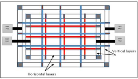
Figure 1: Power Grid Network
The thyristor based static var compensators (SVCs) made up of fixed capacitors and thyristor-controlled reactors can progressively repay reactive power by controlling its terminating points. Nonetheless, during the activity of low-request symphonious flows are produced, which can disintegrate the framework exhibitions.
Power Grid Network
The superposition rule for electrical circuits states that the response (voltage or current) of an immediate system having more than one info shock (independent source) ascends to the logarithmic sum of the responses brought about by each input shock acting alone. The immediate system suggests the electrical circuit contains figuratively speaking independent sources, direct subordinate sources, and straight isolates parts (resistors, inductors, capacitors).
In this work, we acknowledge the trading cells are free current sources, so prepared to regard control grid put together as an immediate structure. A control grid organize show is showed up in Figure 1. The upper arrange is the control organize given by VDD, while the lower orchestrate is the ground orchestrate given by VSS. The ongoing sources are trading cells (reasoning entryways). Thus, the superposition rule is suitable to the immediate control grid arrange illustrate.
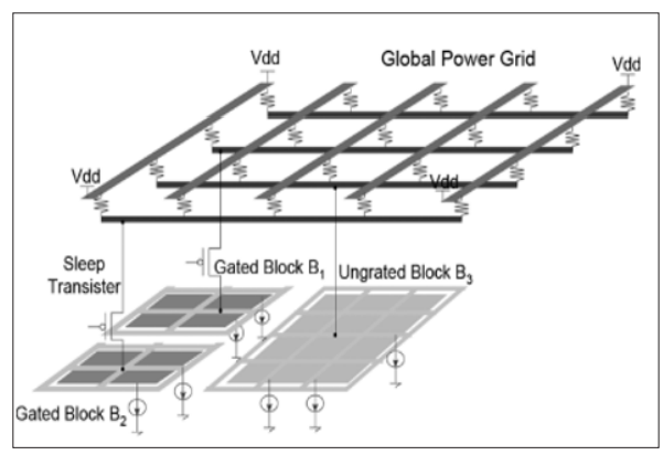
Figure 2: Power Gated Grid Network
In a multi-facet system, control tracks on each metallization layer run the total pass on and are symmetrical to the tracks in adjacent layers. By implies of clusters at the track crossing focuses relate the tracks in connecting layers. Figure 2 appears a numerical depiction besides, demonstrate of the vias. Vias are tended to as assurances whose values depend upon their perspectives. The around the world control grid network is expecting to provide supply voltage to each one of its pieces interior a allowed degree of IR drop and with current densities that fulfill the EM goals on the cross section branches and vias.
Designers of noteworthy remove control transmission systems have ceaselessly known almost the I2R mishap, and take appropriate measures to restrain the incident and overhaul the allotment viability. A given sum of electric control can be sent through a transmission line either at moo voltage and high current, or at the next voltage and lower current. At the point when tall transmission voltage is utilized, transformers near to the client location change over the voltage to a sensible lower voltage.
Since the control misplaced in transmission wires is relative to the direct hindrance and the square of the current, utilizing current at tall voltage diminishes the vitality misplaced as escalated delivered in guides. As demonstrated by Joule's Direction, vitality incident is direct proportional to the square of the current. For occasion, raising the voltage by a component of 10 reduces the progressing by a comparable variable what's more, thus the I2R incident diminishes by a variable of 100, gave comparable evaluated guides are utilized within the two cases. This extension in voltage is for the most part finished in AC circuits by utilizing a move forward transformer. High-voltage coordinate current (HVCC) is utilized to communicate a part of control over critical separations, or on the other hand for interconnects between nonconcurrent frameworks.
Network Analysis
Power arranging means to give capacity to the each large scale, standard cells, and any remaining cells are available in the plan. Power and Ground nets are typically spread out on the metal layers. In this make power and ground structure for both IO cushions and center rationale. The IO cushions power and ground transports are incorporated into the actual cushion and will be associated by projection.
For center rationale there is a center ring encasing the center with at least one arrangements of force and ground rings. The following thought is to build cell power and ground that is inside to center rationale these are called power and ground stripes that rehash at customary spans across the rationale or indicated locale, inside the plan. Every one of these stripes run both in an upward direction and evenly at ordinary stretch then this is called power network.
The complete number of stripes and span distance is exclusively reliant upon the ASIC center power utilization. As power utilization (static and dynamic) expands the distance of force and ground lashes span increment to lessen in general voltage drop, subsequently further developing execution. Notwithstanding the center power and ground ring, large scale power and ground rings should be made utilizing vertical and flat metal layers. A full scale ring walls one in or more macros, totally or somewhat with at least one arrangements of force and ground rings. It is emphatically prescribed to check for power and ground availability after development of the whole PG organization.
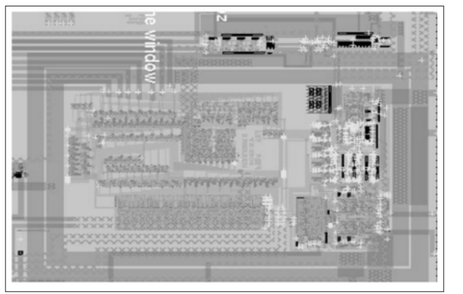
Figure 3: Layout of Grid
Standard cell are put in succession since they are setting next to each other they are contacting one another, and even directing across the cells previously finished so you don't need to anything it resembles a persistent line. That is the reason we are setting filler cells assuming any hole is from there on streamlining.
DC-DC Linear Converter or Regulator
The linear regulator produces a DC output voltage of lower amplitude and of the same polarity than the DC input voltage. They use a resistive voltage divider and have inherently low efficiency, especially if the input to output voltage ratio is high. They are found in a variety of integrated circuits due to their simple design, low circuit complexity, and small area compatibility with on-chip implementation.
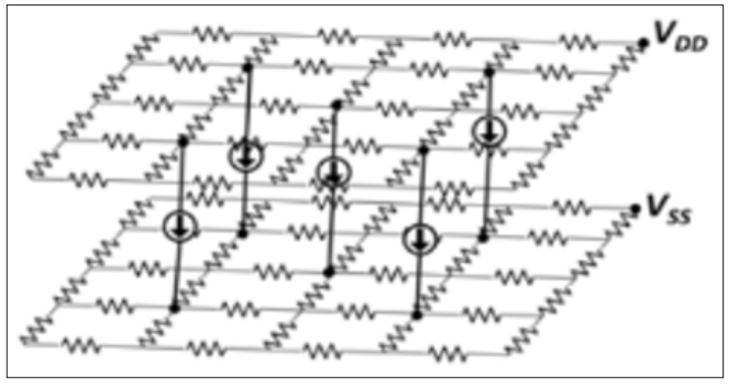
Figure 4: Power and Ground Network
Capacitor DC-DC Converter or Regulator
Capacitor DC-DC Converter(or Load Pump) generates a DC output supply voltage of varying magnitude and/or opposite polarity. relative to the DC input supply voltage. They contain a charge pump and are widely used in integrated circuits to vary the amplitude and/or polarity of the system's main supply voltage. Similar to the linear regulator, the efficiency of the switched capacitor converter is generally low. Additionally, the area occupied by the switched capacitor regulator is larger than that of the linear regulator.
Benefits
The proposed conspire brings down the ongoing move through the dissemination organization to a small portion of its ordinary worth by moving forward the stockpile voltage. This current decrease enjoys expected benefits as recorded underneath.
Power Saving and Expanded Effectiveness
The first and the most expected compensation from a potential execution of this conspire is power saving. We have seen from Joule's Regulation that resistive power misfortune (I2R) has a quadratic connection with current. Likewise, because of the law of preservation of energy, with ideal DC-to-DC converters moving forward the stockpile voltage n times ought to give us power decrease of 1n2. With non-ideal DC-to-DC converters this power saving will be less. In any case, with DC-to-DC converters having nice proficiency, we can in any case anticipate huge decrease in power misfortune over the organization. At the end of the day, power effectiveness of chips will increment tremendously. Moreover, the proposed technique is additionally expected to mitigate the accompanying issues with present day on-chip PDN.
Diminished IR Drop
As current through the organization lessens to a small portion of its unique worth, IR voltage drop across the organization would naturally diminish. In addition, with the DC-to-DC converters nearby loads, the general issue of a heap getting the expected voltage for ideal execution would most likely become unimportant. Anything voltage drop happens across the hubs, the converter would guarantee that a heap is taken care of with ideal stock voltage, e.g., VDD = 1V.
Decreased Electromigration
Through diminished current the proposed plan ought to likewise lighten the electromigration issue in the power circulation organization. Diminished Signal Defer
Vulnerability
As our plan lessens IR drop, the sign postpone vulnerability ought to likewise move along. Diminished Commotion Edge Corruption: By lessening IR drop across the organization, the proposed plan ought to diminish the debasement of clamor edges for on-chip signals.
Conclusion
This paper proposes a programmed strategy to analyze dangerous cells that are answerable for PNS infringement. This instrument additionally recommends a powerful ECO strategy (either resize or move) to perform on hazardous cells to fix PNS infringement. We apply superposition standard and model the PNS finding issue as a direct programming issue. We consider not just PNS requirements yet additionally timing imperatives to ensure that our ECO doesn't causing timing infringement. With our analysis result, architects can perform ECO with very little exertion. The trial results demonstrate the way that we can fix all PSN infringement with just under 3% of all up-and-comer cells [1-9].
References
- Dash S, Baishnab KL, Trivedi G (2019) Applying River Formation Dynamics to Analyze VLSI Power Grid Networks. 29th International Conference on VLSI Design and 2016 15th International Conference on Embedded Systems 258-263.
- Li YC, Lin SY, Lin HY, Li JCM (2018) Diagnosis and Repair of Cells (DRC) Responsible for Power-Supply-Noise IEEE 1-4.
- Shihab MM, Agrawal VD (2019) Energy Efficient Power Distribution on Many-Core 32nd International Conference on VLSI Design and 2019 18th International Conference on Embedded Systems (VLSID) 488-493.
- MacLean E, Jain VK (2011) A Power Transmission Line Fault Distance Estimation VLSI Chip: Design and Defect IEEE International Symposium on Defect and Fault Tolerance in VLSI and Nanotechnology Systems 243- 251.
- Todri A, Sadowska MM (2011) Reliability Analysis and Optimization of Power-Gated ICs. IEEE Transactions on very large scale integration (VLSI) systems 19: 457-468.
- Dash S, Bangera V, Kumar VBY, Trivedi G, Patkar SB (2015) Parallel Two Step Random Walk Algorithm to Analyze VLSI Power Grid IEEE 1-2.
- Wang L, Lam CS, Wong MC (2017) Design of a Thyristor Controlled LC Compensator for Dynamic Reactive Power Compensation in Smart Grid. IEEE Transactions on Smart Grid 8: 409-417.
- Feng Z (2014) Fast RC Reduction of Flip-Chip Power Grids Using Geometric Templates. IEEE Transactions on very large scale integration (VLSI) systems 22: 2357-2365.
- Sharma K (2020) Power planning. VLSI- Physical Design for Freshers. https://physicaldesign4u.com/2020/01/power-planning.html