Author(s): Shakib Alsowidy*, Gobran N Ali and Sahar Slman
The effect of annealing conditions in terms of temperature and time on the structure growth of Sn- 5wt%Sb pritectic solder alloy has been investigated for thirteen samples. These samples were melted at 650°C, and treated at 50, 70,and 100°C for 2,4,6 and 8 hours. The microstructure observation before and after heat- treatment has been studied using X-ray diffraction and optical microscope techniques. The Results showed that, there are two major phases, β- Sn tetragonal solid- solution and SbSn hexagonal intermetallic compound phases. The parameters of microstructure in detailed were accurately determined. At higher aging time there is a little shifting toward a small angle of diffraction and the peaks became sharper. This means that at larger aging time, the d-spacing is greater than that at low aging time, especially for the lines (200),(101),(211),(112),(301) and (420). This may be attributed to the preferred orientation of the structure growth. Also, the particle size and micro-strain change with time for all temperatures examined. The changes in the particle size
and grain boundaries were observed by increasing temperature and time. This is attributed to the recovery and crystalline growth processes with preferred orientations. The reduction in dislocation density has been observed with increasing aging time and temperature. In the heat-treatment process, the changes in microstructure are strongly depending on the variations in dislocation density. As time increases, the more equilibrium phase-distribution is observed
Soldering is the most important joining technology in the electronic industries [1]. During the soldering process, solders are heated and melted first. Liquid (solder)/solid (substrate) connections are generated when molten solders wet the substrates. The solders solidify and solder joints are produced when the joints have been cooled. Solders are typically had low melting point alloys since melting is necessary in the soldering process.
Sn-Pb solder alloys have long been thought to be the most extensively utilized material for joining and packaging electronic components. This is attributed to the following properties: low cost, low melting temperature 183°C, good manufacturability, Acceptable mechanical properties, good wettability, and Reliability
Despite these benefits, owing to the intrinsic toxicity of Pb, a surge in research towards finding a suitable lead-free solder (LFS) has emerged. Cu, Ag, Zn, Bi, Sb, Ni, In, Ge, Al, and Cr can be utilized in lead-free soldering [2]. However, because of worring about the toxicity of Pb, limitations on its usage in solder alloys have been introduced. In reality, the European Union (EU)has enacted legislation known as Restrictions Of Hazardous Substances (ROHS) Directive, which restricts the maximum content Pb solder alloys to 0.1 percent by weight on all electronic products entering the EU market as of July 2006. Lead particles in the environment can attach to dust and be carried long distances in the air. Such lead-containing dust can be removed from the air by rain and deposited on surface soil where it may remain for many years. In addition, heavy rains may cause lead in surface soil to migrate into ground water and eventually into water systems [3].
The 13 samples of pertictic Sn-5wt.%Sb were prepared by mixing 95 wt% of high - purity tin (99.999%) and 5 wt% of high-purity antimony (99.999%) and melted at 650°C. During heating and to obtain a uniform distribution of molten constitutes and materials, continuous vibration has carried out during melting using flask shake. After completely melting, the samples were directly cold in ice in order to prevent any equilibrium transformation or equilibrium structure. After that the cast ingot was polished and washed to remove the loosely adherent precipitate during melting and to remove residual stress and defects using grades of silicon paper and by acetone solution. The cast ingot obtained was cold -drawn into four main sheet groups with a thickness of 1mm and divided into thirteen samples.
The heat treatment process was performed using the digital electric furnace that has a temperature scale from 1°C to 250°C. The samples were divided to four groups (A0, B, and C) and treated at 50, 70 and 100°C for 2,4,6 and 8 hours with slowly cooled in furnace to room temperature (RT) with a cooling rate of (- 0.2)°C /min
In order to investigate and follow the variations of microstructure that might be occurred during and after heat treatment. XRD and optical microscopy have been conducted.
The x-ray diffraction is a common characterization technique which is used to determine phase structure that found in the materials. Figures. (1a, b, c) show the x-ray diffraction patterns obtained for the treated samples at various temperatures 50, 70,100°C, respectively.
From these patterns, there are two main phases, β- Sn tetragonal matrix phase and SnSb hexagonal structure phase. The major phase is β-Sn phase as can be seen form the intensity of the peaks. Using the Jade 6.5 software Program, the data obtained have been compared with the Standard data according to the Joint Committee on Powder Diffraction Standards at International Center for Diffraction Data (JCPDS-ICDD). From the patterns obtained it can be concluded that the Sb-phase is not found in the structure and this means that the Sb-content has reacted with Sn atoms to form SnSb (IMC) and the remaining atoms dissolved in the β-Sn solid solution. The same result has been shown for all treated samples.
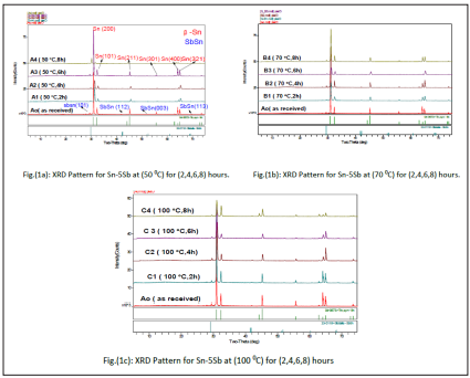
The displacement between atomic levels was extract from XRD- Patterns and calculated Using Brags law equation. From figure (1 a, b, c), it can be seen that the effect of heat treatment is very clear. As increasing aging time there is a little shifting toward a small angle of diffraction and the peaks became sharper. This means that at 50°C and large aging time, the d-spacing is greater than that at low aging time. This is more pronounced for lines (200), (101), (211), (112),(301) and (420). At different orientation, d-spacing has been calculated and plotted as a function of time and temperature as can be shown Figure (2) and table (1). From this Figure the sample aged at 50°C exhibits different behavior when comparing with other samples. The d- spacing increases with increasing aging time for the line (200). This behavior is the same for all lines (101), (211), (301), (112) and (420). This increase means that there is a shifting in the diffraction angle to the left in the XRD-Pattern. Besides the significant shifting in the diffraction angle there is a deformation of peaks with increasing aging time.
| Aging time (h) | d(A) (Aging at 50°C) | d(A) (Aging at 70°C) | d(A) (Aging at 100°C) |
|---|---|---|---|
| 2 | 2.8537 | 2.8733 | 2.8843 |
| 4 | 2.8482 | 2.8751 | 2.8750 |
| 6 | 2.8860 | 2.8589 | 2.8824 |
| 8 | 2.959 | 2.8715 | 2.8786 |
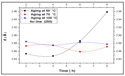
Figure 2: d- Spacing as Function of Time for Line(200)
For the samples B and C there is no change observed in the d-spacing with aging time. The small limited change observed may be due to the approximation in calculation processes. In general, from the observation of Sn-Sb phase diagram, in the temperature range from 0 the 120°C there is no any phase- transition in this temperature range.
The influence of aging temperature on grain size of the two phases, β-Sn and SnSb (IMC), was calculated by Debye-Scherre'r formula [10],

Where β: is the full width at half maximum in radian, θ is the Bragg's angle, and is the wavelength of X-Ray used (1.54056 A0 ). From the comparison between XRD curves in figure 1, it can be seen that β-Sn grains does not clearly affected by aging especially at 50°C. Form figure 1, it is clear that as aging temperature increased there is some peaks diminishes and some other become more large in intensity and sharpness lines. The complete analysis of the individual patterns was performed to obtain an average grain size as a function of heat treatment condition as shown in Table (2) and Figure (3a).
Table 2: Particle Size as Function of Time for all Samples
| Aging time (h) | Particle Size (A) Aging at 50°C | Particle Size(A) Aging at 70°C | ParticleSize(A) Aging at 100°C | Particle Size(A) For Ao (As-received) |
|---|---|---|---|---|
| 2 | 292.5785 | 293.6605 | 604.2177 | 445.59162 |
| 4 | 363.0522 | 608.4042 | 580.7835 | |
| 6 | 526.2681 | 315.7331 | 343.3695 | |
| 8 | 480.6829 | 502.64892 | 297.8660 |
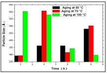
Figure 3a: Particle size as Function of Aging Time for Samples
From table (2) and Figure (3), the changes in particle size and microstrain during heating are shown for different time intervals. These results refer with an increased temperature, the passage of atoms from one convex grain in a neighboring grain through the boundary occurs and continues [4]. In this coarsening process some grains diminish in size and even disappear while others become larger and devour adjacent grains. This growth in grain size is accelerated with increasing temperature as shown in table (2) and Figure (3a). The higher the temperature of aging, the larger the recrystallized grains [6]. The fluctuation in the values of average particle size may be attributed to the inverse behavior of the Hall-Petch equation [8]. The K parameter is often positive and related to the microstructure refinement ( < 1μm). In this case, the positive normal behavior is the mechanism of strengthening of the material [9]. As the annealing temperature increases, grain growth accelerates. Then the K-parameter becomes negative and the inverse behavior of the Hall-Petch relation is the dominant mechanism. This is demonstrated and reported by various literature [9]. Figure (3b,c) showed the variation in the volume fraction of SnSb IMC with annealing temperature. It can be seen that the precipitated SnSb particle size increases with increasing temperature at all times examined. This means that the β-Sn structure size is reduced as temperature increased to 100°C. The above observations besides the preferred orientation of particles all explain the changes in size of particles observed.
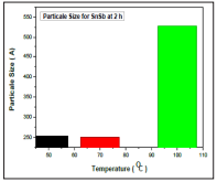
Figure 3b: Particle Size as Function of Aging Time
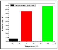
Figure 3c: Particle size as Function of Aging Time for Samples
To obscene the influence of heat-treatment. On the microstructure of Sn-5wt%Sb solder alloy, we perform services measurements at temperatures ranging from room temperature to 0.4Tm for different aging time (from 2h to 8h). Figure (4) show the OM images and phase distribution of as -cast Sn- 5wt%Sb and after heat- treatment.
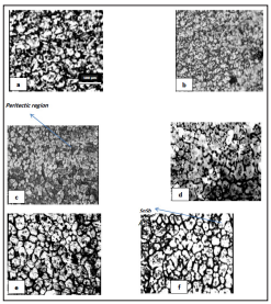
Figure 4: OM Images for the Samples, (a, b) -as Received, (c, d) Treated at (2h, 50°C), (e, f ) - Treated at ( 8h, 100°C)
As can be seen form these two Figures, large bright - gray and very fine dark-gray regions with sub-micrometer scales were observed. The bright-gray area with a flower structure isthe β-Sn matrix phase and the dark-gray areas are fine SnSb (IMC) precipitated phase particles. This flower structure regime becomes more pronounced as aging time increases which is evidence for the equated and uniform microstructure. The images refer that after heat-treatment the microstructure becomes larger in size and uniformly distributed especially at higher temperature as shown in Figure (4b, c). The combined results of XRD and OM indicate that the aging temperature makes the microstructure coarser and less defects. These variations in microstructure may be attributed to the strain-relief crystallization process of a cold - worked alloy [5]. The strain - relief crystallization of a cold - worked alloy is the process at which the number of defects decreases since the positive dislocation interacts with the negative one and results in a noticeable decrease of dislocation density as can be seen from OM images in Figure (5). In this process and during aging, any increase in temperature accelerates the movement of points and linear crystal defects and so provides favorable conditions for redistribution of dislocations and reduction of their density. Redistribution of dislocations involves a release of residual stresses and increase the alloy density [7]. So, it is clear that the heat- treatment, especially at 50 to 70°C, leads to obtaining a homogeneous, uniform and stable grain structure.
In the present work, the effect of annealing conditions in terms of temperature and time on the structure growth of Sn- 5wt.%Sb pritectic solder alloy has been investigated. The results are summarized as follows: